

Semiconductors Fabrication
Environmental Relevance of the Semiconductor Industry
Semiconductors play a pivotal role enabling progress while reducing the associated environmental impact.

In a world experiencing continuous population growth, rising standards of living, and accelerating industrialization, semiconductors play a pivotal role as foundational technologies enabling progress while reducing the associated environmental impact. Semiconductors, primarily composed of silicon-based materials, have been instrumental in driving the Third Industrial Revolution of the 1970s – characterized by the rise of the first computers – and are now central to the ongoing Fourth Industrial Revolution, marked by extensive digitalization, artificial intelligence, and the Internet of Things (Fig. 1). At the core of these revolutions are transistors, which are microscopic semiconductor devices acting as electrical switches, interconnected to form increasingly complex hardware capable of performing sophisticated tasks. Electronic components based on state-of-the-art semiconductor systems are key enablers of advanced technology across a number of applications. These components are often engineered to reduce their own environmental footprint, such as through improved energy efficiency, but also to facilitate a broad spectrum of sustainable technologies. For example, power electronics is a fundamental enabler of vehicle electrification; digital monitoring of industrial operations optimize production processes, leading to resource savings and waste reduction; predictive AI tools can help farmers optimize crop yields and avoid crop loss.
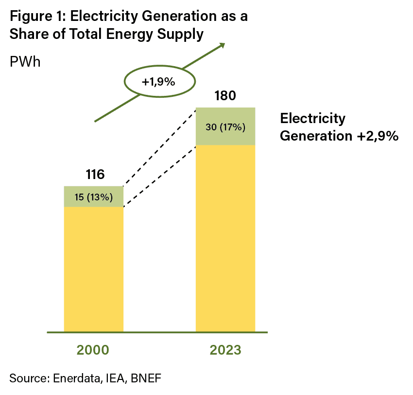
Semiconductors became widespread in large part due to Moore’s Law – the 1965 prediction that transistor density would double each year – leading to dramatic growth in computing power and unlocking increasingly diverse technological capabilities. (Fig. 1). The development of this industry therefore intrinsically follows a principle of resource efficiency, pursuing continuous performance enhancement while minimizing resource consumption, thus serving as a cornerstone for both technological advancement and environmental sustainability. This evolution has split the semiconductor market into two main segments.
Today, approx. 30% of the market consists of advanced, continually miniaturized technologies (leading nodes) used predominantly in high-performance computing (such as
data centers processors), advanced telecommunications equipment, and high-end consumer electronics (e.g., premium laptops, tablets and smartphones). The larger share comprises more mature, larger transistors (lagging nodes) utilized across automotive, industrial applications, and mid- to low-end consumer electronics (such as mid-range smartphones and home appliances).
A single semiconductor production facility can consume up to 38 million liters of ultrapure water a day – equivalent to the daily water consumption of c. 260,000 European citizens.
Despite embedding strong positive environmental principles, the semiconductor industry is also associated with sizeable negative impacts. Miniaturization relies on complex manufacturing processes that transform silicon ingots, typically 2 meters long and 30 centimeters wide, into functional transistors measured in nanometers to micrometers. These complex production processes demand substantial resources, including significant amounts of raw materials, chemicals, water, and energy. Water consumption represents one of the most pressing environmental issues within semiconductor fabrication, as a single production facility can consume up to 38 million liters of ultrapure water daily—equivalent to the daily water consumption of approximately 260,000 European citizens. Energy consumption is similarly extensive, projected to reach 237 TWh by 2030, roughly forty times Milan’s annual energy demand. The industry’s negative environmental impact also extends to product usage. Enhanced efficiency and economic convenience of electronic components trigger the Jevons’ paradox, which describes how improved efficiency reduces usage costs, thus increasing demand to the point of facilitating overconsumption patterns. Additionally, the industry significantly contributes to electronic waste—approximately 74 million tons per year—with only about 17% adequately recycled.

In this context, while not all semiconductor companies can be considered as having a net positive environmental impact, there are three distinct ways in which semiconductor companies contribute to positive environmental outcomes:
1. Advanced technologies: companies for which miniaturization is a solid growth driver, resulting in continuous resource efficiency improvement. Companies that lie within this category are typically listed players, positioned across the whole value chain, including design houses, foundries and equipment manufacturers, that lead the global technological innovations by setting industry standards;
2.Positive end market applications: companies that manufacture state-of-the-art electronics whose applications revolve around resource efficiency or pollution control systems, such as power electronics enabling electrification of the economy or enabling greater efficiency gains in electricity conversion, or sensors used in measuring polluting agents;
3.Process optimization: Service and product companies whose business is to mitigate the negative environmental effects associated with semiconductor production itself. For instance, testing technologies or advanced cleanroom facilities reduce electronic waste by preventing defective components from reaching the market and causing larger damage.
Investment opportunities
The semiconductor industry is projected to grow from c. $600 billion to $1 trillion by 2030.

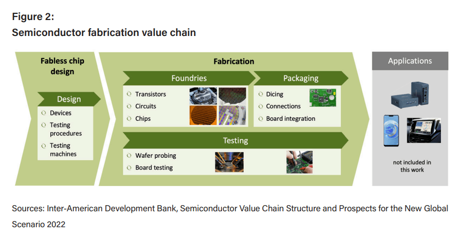
The semiconductor industry presents an attractive investment opportunity, projected to grow from approximately $600 billion to $1 trillion by 2030, achieving a CAGR of roughly 10% (Fig. 1).
This growth is propelled by digitalization, industrial automation, and the extensive adoption of consumer electronics.
From a public markets investment standpoint, the semiconductor value chain (Fig.2) can appear highly consolidated, dominated by listed companies benefiting from strong competitive advantages such as high capital expenditures, economies of scale, and extensive R&D capabilities. At a high level this is true, and several key areas are actually oligopolies. Environmentally, these companies drive innovation and set global standards in electronics development. Fabless design companies, like NVIDIA and Qualcomm, remain agile market leaders, supported by Electronic Design Automation (EDA) firms such as Cadence and Synopsys, which enhance design precision and reliability. Foundries, such as TSMC, Samsung, and GlobalFoundries, along with vertically integrated giants like Infineon, Intel, NXP, and STMicroelectronics, encompass critical production capabilities. Equipment manufacturers, including ASML, Lam Research, and Applied Materials contribute significantly to newer, more efficient technologies, being the very first enablers of miniaturization. Testing and packaging specialists such as Advantest, Amkor, and Technoprobe, complete this robust public markets investment landscape, with the critical role of ensuring high quality of the final products.
On the Private markets side, in contrast, there are several niches below the surface which are still fragmented and comprise numerous small players, frequently startups or family-run businesses closely linked to local listed companies.
In a global semiconductor landscape largely dominated by Asian and American companies, Europe maintains a unique position, excelling particularly in semiconductor equipment manufacturing and semiconductors for the industrial and automotive end markets. Notable European semiconductor clusters include Dresden in Germany, centered around Infineon and Bosch, Grenoble-Rousset in France, northern Italy and Sicily, anchored by STMicroelectronics, the Netherlands ecosystem linked to ASML and NXP, heritage of Philips, and specialized R&D hubs in the UK, collaborating primarily with Intel.
The most compelling investment opportunities in the private market space fall within three categories:
- Technological disruptions: New materials used or new applications for existing technologies where less consolidated players have a competitive advantage in their agility. Examples are the shift to silicon carbide (SiC) and gallium nitride (GaN) devices, critical for advanced power electronics, or revolutionary devices such as Micro Electro Mechanical Systems (MEMS) impacting sensor technology. Manufacturers of equipment for these technologies also fall within this category;
- Specialized niche providers: Companies delivering advanced, highly specialized semiconductor design or testing solutions tailored to specific applications;
- Local service champions: Providers of critical infrastructure services such as cleanroom and HVAC system installations and maintenance, crucial for achieving precise manufacturing environments and defect-free semiconductor production.